

SYKJ2302A_SOT23_N_耐压20V_电流3.6A_VGS±12V
-


SYKJ2302A
« Green Device Available
« Super Low Gate Charge
« Excellent Cdv/dt effect decline
« Advanced high cell density Trench technology
The SYKJ2302A is the high cell density trenched N-ch MOSFETs, which provides excellent RDSON and efficiency for most of the small power switching and load switch applications.
The SYKJ2302A meet the RoHS and Green Product requirement with full function reliability approved.
SYKJ2302A_EN_V01
第 1/6页
深圳市双宜科技有限公司
Symbol
Parameter
Typ.
Max.
Unit
RθJA
Thermal Resistance Junction-ambient 1
---
112
℃/W
RθJC
Thermal Resistance Junction-Case1
---
---
℃/W
Thermal Data
Symbol
Parameter
Rating
Units
VDS
Drain-Source Voltage
2 0
V
VGS
Gate-Source Voltage
±12
V
ID@TA=25℃
Continuous Drain Current, VGS @ 10V1
3.6
A
ID@TA=70℃
Continuous Drain Current, VGS @ 10V1
1.5
A
IDM
Pulsed Drain Current2
12
A
PD@TA=25℃
Total Power Dissipation3
1.05
W
TSTG
Storage Temperature Range
-55 to 150
℃
TJ
Operating Junction Temperature Range
-55 to 150
℃
Absolute Maximum Ratings
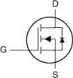
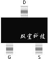
SOT23 Pin Configuration
Description
BVDSS
RDSON
ID
20V
35 mΩ
3.6 A
Product Summary
SYKJ2302A
Electrical Characteristics
TC = 25°C unless otherwise noted
Off Characteristics
On Characteristics
Dynamic Characteristics
Switching Characteristics
Drain-Source Diode Characteristics and Maximum Ratings
Notes:
1. Repetitive Rating: Pulse Width Limited by Maximum Junction Temperature
2. Device mounted on FR-4 PCB, 1inch x 0.85inch x 0.062 inch
3. Pulse Test: Pulse Width≤300μs, Duty Cycle≤0.5%
SYKJ2302A_EN_V01
第 2/6页
深圳市双宜科技有限公司
IS
Maximum Continuous Drain-Source Diode Forward Current
--
--
3.5
A
ISM
Maximum Pulsed Drain-Source Diode Forward Current
--
--
10.5
A
VSD
Drain to Source Diode Forward Voltage,V GS = 0V, I SD =3.5A,T J = 25℃
--
--
1.2
V
td(on)
Turn-On Delay Time
VGS=5 V, VDS=10V, ID =3A, RG = 6 Ω ,RL = 2.7 Ω
--
4.5
--
ns
tr
Turn-On Rise Time
--
31
--
ns
td(off)
Turn-Off Delay Time
--
12
--
ns
tf
Turn-Off Fall Time
--
4.0
--
ns
Qg
Total Gate Charge
VDS = 10 V, ID =3A, VGS = 5V
--
6.23
--
nC
Qgs
Gate-Source Charge
--
6
--
nC
Qgd
Gate-Drain Charge
--
0.5
--
nC
Ciss
Input Capacitance
VDS = 10V, VGS = 0 V, f = 1.0 MHz
--
180
-
pF
Coss
Output Capacitance
--
37
-
pF
Crss
Reverse Transfer Capacitance
--
34
-
pF
VGS(th)
Gate Threshold Voltage
VDS = VGS, ID = 250 uA
0.45
-
1.1
V
RDS(on)
Static Drain-Source On-Resistance
VGS = 4.5 V, ID =3.5A
--
35
45
mΩ
VGS = 2.5 V, ID =2.0A
-
46
57
BVDSS
Drain-Source Breakdown Voltage
VGS = 0 V, ID = 250 uA
20
--
--
V
IDSS
Zero Gate Voltage Drain Current
VDS =20 V, VGS = 0 V
--
--
1
uA
VDS = 16V, TC = 125℃
--
--
10
uA
IGSSF
Gate-Body Leakage Current, Forward
VGS = 10V, VDS = 0 V
--
--
100
nA
IGSSR
Gate-Body Leakage Current, Reverse
VGS = -10 V, VDS = 0 V
--
--
-100
nA
Symbol
Parameter
Test Conditions
Min
Typ
Max
Units
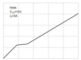
Note: VDS=10V, ID=3A
SYKJ2302A
Typical Performance Characteristics
N- Channel Typical Characteristics
4
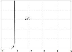
2.0V
1.5V
5
4
TC=25℃
impulse=250uS
2.5V
3
10V
25℃
3
2
2
1.2V
1
1
1.0V
0
0
0
1
2
3
4
5
0
1
2
3
4
5
Vds Drain-Source Voltage (V)
Figure 1. On-Region Characteristics
Vgs Gate-Source Voltage (V)
Figure 2. Transfer Characteristics
100
3.5
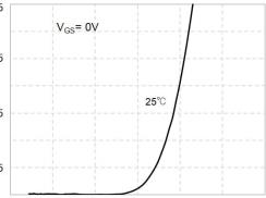
Note:TJ=25℃
VGS= 0V
80
2.5
60
VGS=2.5V
25℃
1.5
40
VGS=4.5V
20
0.5
0
0
0
0.2
0.4
0.6
0.8
1.0
1.2
0
1
2
3
4
V F ,Forward Voltage [V]
Figure 4. Body Diode Forward Voltage Variation with Source Current
and Temperature
I D - Drain Current (A)
Figure 3. On-Resistance Variation vs Drain Current and Gate Voltage
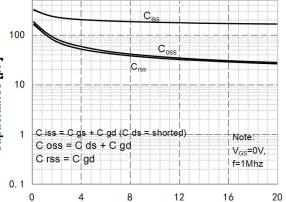
5
Ciss
4
Coss
Crss
3
2
C iss = C gs + C gd (C ds = shorted)
C oss = C ds + C gd C rss = C gd
Note: VGS=0V,
f=1Mhz
1
0
0
1
2
3
4
5
VDS
Drain-to-Source Voltage (V)
Qg Gate Charge (nC)
Figure 6. Gate Charge Characteristics
Figure 5. Capacitance Characteristics
SYKJ2302A_EN_V01
第 3/6页
深圳市双宜科技有限公司
Rdson On-Resistance(mΩ)
ID - Drain Current (A)
Capacitance [pF]
Vgs Gate-Source Voltage (V)
I D - Drain Current (A)
IF Forward Current (A)
5
5
5
SYKJ2302A
N- Channel Typical Characteristics
0.7
(Continued)
1
0.6
0.8
0.4
0.6
0.3
0.4
0.2
0.1
0
0
0
2
4
6
8
10
12
0
3
6
9
12
15
Vgs Gate-Voltage (V)
Figure 7. Breakdown Voltage Variation vs Gate-Voltage
Vgs Gate-Voltage (V)
Figure 8. On-Resistance Variation vs Gate Voltage
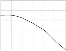
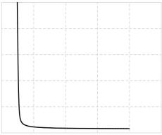
100
5
10
10μs
4
100μs
1ms
3
10ms
1
100ms
Limited by RDS(on)
2
DC
0.1
1
TC=25℃
Note: TC=25℃,
TJ=150℃,Single pulse VDS (V)
0
0.01
0
25
50
75
100
125 150
0.1
1
10
20
100
Vds Drain-Source Voltage (V)
Figure 9. Maximum Safe Operating Area
T J -Junction Temperature(℃)
Figure 10. Maximum PContinuous Drain Currentvs Case Temperature
100
-1
10
D = 0 . 5
D = 0 . 2
t1
D=0.1
t2
D = 0 . 0 5 D = 0 . 0 2
10-2
D=0.01
Notes:
Single pulse 1.Dty factor D=t1/t2
2.Peak TJ=PDM*ZthJC+T
TP(s)
-2
10
10
-3
C
-5 -4 -3
10 10 10
1
10
2
10
3
10-6
10
Square Wave Pluse Duration(sec)
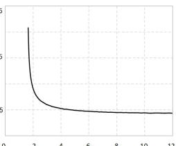
Figure 11. Transient Thermal Response Curve
SYKJ2302A_EN_V01
第 4/6页
深圳市双宜科技有限公司
r(t),Normalized Effective Transient Thermal Impedance
Voltage(Normalized) -BVDSS Drain-Source Breakdown
I D - Drain Current (A)
PDM
RDS(ON),(Normalized)
Drain-Source On Resistance
ID - Drain Current (A)

SYKJ2302A
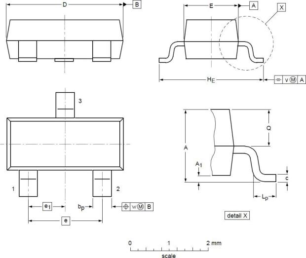
SOT23 Mechanical tData
DIMENSIONS ( unit : mm )
SYKJ2302A_EN_V01
第 5/6页
深圳市双宜科技有限公司
Symbol
Min
Typ
Max
Symbol
Min
Typ
Max
A
0.90
1.01
1.15
A1
0.01
0.05
0.10
bp
0.30
0.42
0.50
c
0.08
0.13
0.15
D
2.80
2.92
3.00
E
1.20
1.33
1.40
e
--
1.90
--
e1
--
0.95
--
HE
2.25
2.40
2.55
Lp
0.30
0.42
0.50
Q
0.45
0.49
0.55
v
--
0.20
--
w
--
0.10
--


声明:
双宜科技保留电路及其规格书的更改权,以便为客户提供更优秀的产品,规格若有更改,恕不另行通知。
Ø
双宜科技一直致力于提高产品的质量和可靠性,然而,任何半导体产品在特定条件下都有一定
的失效或发生故障的可能,客户有责任在使用双宜产品进行产品研发时,严格按照对应规格书的要求使用双宜产品,并在进行系统设计和整机制造时遵守安全标准并采取安全措施,以避免潜在失败风险造成人身伤害或财产损失等情况。如果因为客户不当使用双宜产品而造成的人身伤害、财产损失等情况,双宜公司不承担任何责任。
Ø
本产品主要应用于消费类电子产品中,如果客户将本产品应用于医疗、军事、航天等要求极高
质量、极高可靠性的领域的产品中,其潜在失败风险所造成的人身伤害、财产损失等情况,双宜科技不承担任何责任。
Ø
本规格书所包含的信息仅作为双宜产品的应用指南,没有任何专利和知识产权的许可暗示,如
果客户侵犯了第三方的专利和知识产权,双宜科技不承担任何责任。
关于我们:
深圳市双宜科技有限公司是一家专业从事中低压场效应管、模拟集成电路芯片产品的研制、开发和销售的高新技术企业,自公司2012年成立以来,我们拥有了广大的客户群,本公司主要经营中低压场效应管,MCU设计,电源管理IC,LED驱动IC,触摸控制IC等。公司秉承坚持 " 服务第一,品质第一,客户第一 " 的原则为广大客户提供优质的服务。
客户服务中心:
深圳市双宜科技有限公司电话:0755-27863192
手机:13823527686
网址:双击打开网址了解更多详情
样片、技术支持微信:
SYKJ2302A_EN_V01
第 6/6页
深圳市双宜科技有限公司
-


